Introducción: The Invisible Backbone of Silicon Processing
In the semiconductor industry, a wafer carrier is not just a container; it is a critical component that must withstand aggressive chemicals and strict cleanroom requirements. Any microscopic contamination or dimensional instability during transport can lead to significant wafer loss.
En Rápido, we specialize in high-precision CNC machining of wafer carriers (FOUPs, cassettes, and trays) that meet the rigorous standards of semiconductor fabrication.

Semiconductor Grade vs. General Machining
Machining for the semiconductor sector requires a “zero-contamination” mindset. Here is how we ensure your wafer carriers perform:
| Característica | General Industrial Machining | Rapidefficient Semiconductor Grade |
| Material Purity | Standard grades | High-purity, low-outgassing plastics |
| Tolerance Control | $\pm 0.05$ mm | $\pm 0.01$ mm to $\pm 0.005$ mm |
| Acabado superficial | $Ra$ 1.6 | $Ra$ 0.2 – $Ra$ 0.4 (Ultra-smooth) |
| Cleaning Protocol | Standard degreasing | Limpieza ultrasónica & Cleanroom packaging |
| ESD Control | Often ignored | Certified ESD-safe material processing |
Technical Mastery in Wafer Carrier Fabrication
1. Advanced Material Expertise (OJEADA, Ptfe, and ESD Plastics)
Wafer carriers often face harsh environments. We process specialized materials designed for the “Fab”:
- OJEADA (Victrex 450G): Excellent mechanical strength and chemical resistance.
- Ptfe / PFA: For high-temperature chemical baths where zero corrosion is required.
- ESD-Safe Plastics: Preventing static discharge that could destroy sensitive microcircuits.
2. Managing Thermal Stability and Warpage
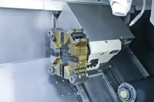
Wafer carriers are often large but thin-walled. Durante el mecanizado CNC, these parts tend to warp due to material memory.
- Nuestra solución: We use custom vacuum fixtures and specialized cooling techniques to ensure that even large-format carriers maintain perfect flatness across the entire surface.
3. Particle Control and Burring Management
In a cleanroom, a single loose burr is a disaster.
- Nuestra solución: Our technicians perform high-magnification manual deburring to ensure all edges are “radiused” and smooth, preventing particle generation during wafer loading.
Frequently Asked Questions (Preguntas frecuentes)
Q: What materials are best for wafer carriers? A: PEEK and PTFE are the most common due to their chemical resistance and low outgassing. For high-temperature applications, we also offer specialized ceramic and quartz machining.
Q: How do you ensure ESD safety during machining? A: We use certified ESD-safe materials and maintain strict control over surface finishes to prevent static build-up during wafer transport.
Q: Can you handle large-format wafer trays? A: Sí, our 5-axis CNC centers can handle large dimensions while maintaining flatness tolerances within microns.
Why Partner with Rapidefficient?
We don’t just deliver parts; we deliver peace of mind for your semiconductor supply chain.
- Full Traceability: Material certifications and inspection reports with every batch.
- DFM for Semiconductors: We help you optimize wall thickness for stability.
- Fast Prototyping: Accelerate your R&D cycle with 3-5 day lead times.
Need a semiconductor-grade solution for your wafer carriers?
[Contact Our Engineering Team for a DFM Review] or explore our [Servicios de mecanizado CNC] for more precision manufacturing solutions.