In the context of the rapid development of today’s high-tech industry, the importance of semiconductor technology as the “brain” of modern electronic devices is self-evident. From smartphones and computers to new energy vehicles and artificial intelligence systems, almost all high-end electronic products rely on high-performance semiconductor chips. In the semiconductor industry chain, an often overlooked but crucial link is CNC semiconductor parts processing. It is not only the basis for ensuring the high-precision operation of semiconductor equipment, but also the key technical support that drives the entire industry towards higher integration, smaller size and stronger performance.
What is CNC Semiconductor Parts Machining?
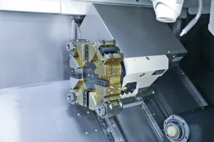
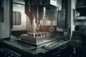
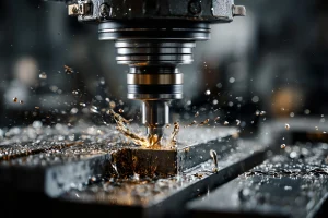
CNC (Computer Numerical Control) machining is an advanced manufacturing process that automatically completes complex cutting tasks by controlling machine tools through preset programs. In the semiconductor field, CNC machining is mainly used to manufacture key components in semiconductor production equipment, such as wafer carrier tables, vacuum chamber components, alignment mechanisms, sensor holders, and high-precision fixtures. These parts often require micron or even sub-micron precision while providing excellent surface finish, thermal stability, and chemical corrosion resistance.
Due to the extremely harsh semiconductor manufacturing environment – such as ultra-high vacuum, high temperature, strong acid and alkali cleaning, etc., extremely high requirements are placed on the material selection and processing quality of the components used. Common machining materials include aluminum alloys, stainless steel, titanium alloys, ceramics, and specialty engineering plastics such as PEEK. CNC technology, with its high repeatability, high degree of automation, and superior precision control, is the ideal solution for meeting these demanding needs.
The core role of CNC machining in semiconductor equipment
1. Ensuring Equipment Stability and Accuracy
Lithography, etching, deposition and other steps in the semiconductor manufacturing process need to be precisely controlled at the nanometer level. Any slight mechanical deviation can lead to the scrapping of an entire batch of wafers. CNC machining ensures that the geometric dimensions of each part are highly consistent, thereby improving the assembly accuracy of the whole machine and reducing system errors.
2. Support Integrated Molding for Complex Structures
The internal structure of modern semiconductor equipment is becoming increasingly compact, and many components require the integration of cooling channels, gas deflection holes, sealing grooves and other functional features. CNC five-axis linkage machining technology can complete complex structural processing of multiple angles and surfaces at one time, reducing assembly links and improving reliability and sealing performance.
3. Shorten R&D cycles and improve production efficiency
With the seamless integration of CAD/CAM software with CNC systems, engineers can complete the entire process from design to sample production in a short time. This is especially important for the rapid iteration of semiconductor equipment development. Additionally, the automation features of CNC machining significantly enhance the efficiency and consistency of mass production.
Technical Challenges and Strategies for Responding
Despite the significant advantages of CNC machining, it still faces many challenges when applied in the semiconductor field:
Thermal Deformation Control: Prolonged cutting generates heat, affecting the dimensional stability of the part. To this end, enterprises often use low-temperature cooling, segmented processing and constant temperature workshop to control it.
Extremely High Surface Roughness Requirements: Some vacuum contact surfaces require a mirror effect of Ra<0.1 μm. This requires a combination of post-processing processes such as precision grinding, polishing, or electrolytic deburring.
Cleanliness Management: Metal dust generated during processing can contaminate the cleanroom environment. As a result, more and more manufacturers are introducing enclosed machining centers with efficient dust collection systems.
Future development trends
With the rise of third-generation semiconductors (such as silicon carbide SiC and gallium nitride GaN) and the development of advanced packaging technologies (such as chiplet and 3D packaging), higher requirements have been put forward for CNC machining. Future trends will focus on the following aspects:
Popularization of ultra-precision CNC machine tools with higher precision;
Intelligent monitoring system integration to achieve real-time feedback and optimization of the processing process;
In-depth green manufacturing concept, promotion of energy-saving tools and recyclable cutting fluid technology;
Integration with additive manufacturing (3D printing) to form a new “mix-and-match” manufacturing model.
Epilogue
Although CNC semiconductor parts processing is behind the scenes, it is the “invisible hero” that supports the steady progress of the entire semiconductor industry. It not only reflects the pursuit of ultimate precision in modern manufacturing, but also highlights China’s continuous breakthroughs in the field of high-end equipment manufacturing. With the acceleration of the autonomy of domestic semiconductor equipment, enterprises that master core CNC machining technology will occupy a more advantageous position in global competition. In the future, only by continuous innovation and excellence can we go further and more steadily on this road to the microscopic world.