Introduzione: The Invisible Backbone of Silicon Processing
In the semiconductor industry, un portawafer non è solo un contenitore; it is a critical component that must withstand aggressive chemicals and strict cleanroom requirements. Any microscopic contamination or dimensional instability during transport can lead to significant wafer loss.
A Rapido, we specialize in high-precision CNC machining of wafer carriers (FOUPs, cassettes, and trays) that meet the rigorous standards of semiconductor fabrication.

Semiconductor Grade vs. General Machining
Machining for the semiconductor sector requires a “zero-contamination” mindset. Here is how we ensure your wafer carriers perform:
| Caratteristica | General Industrial Machining | Rapidefficient Semiconductor Grade |
| Material Purity | Standard grades | High-purity, low-outgassing plastics |
| Tolerance Control | $\pm 0.05$ mm | $\pm 0.01$ mm to $\pm 0.005$ mm |
| Finitura superficiale | $Ra$ 1.6 | $Ra$ 0.2 – $Ra$ 0.4 (Ultra-smooth) |
| Cleaning Protocol | Standard degreasing | Pulizia ad ultrasuoni & Cleanroom packaging |
| ESD Control | Often ignored | Certified ESD-safe material processing |
Technical Mastery in Wafer Carrier Fabrication
1. Advanced Material Expertise (SBIRCIARE, PTFE, and ESD Plastics)
Wafer carriers often face harsh environments. We process specialized materials designed for the “Fab”:
- SBIRCIARE (Victrex 450G): Excellent mechanical strength and chemical resistance.
- PTFE / PFA: For high-temperature chemical baths where zero corrosion is required.
- ESD-Safe Plastics: Preventing static discharge that could destroy sensitive microcircuits.
2. Managing Thermal Stability and Warpage
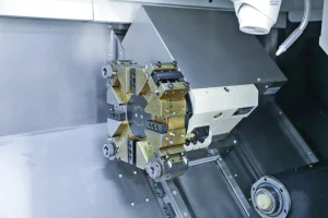
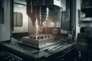
Wafer carriers are often large but thin-walled. Durante la lavorazione CNC, these parts tend to warp due to material memory.
- La nostra soluzione: We use custom vacuum fixtures and specialized cooling techniques to ensure that even large-format carriers maintain perfect flatness across the entire surface.
3. Particle Control and Burring Management
In a cleanroom, a single loose burr is a disaster.
- La nostra soluzione: Our technicians perform high-magnification manual deburring to ensure all edges are “radiused” and smooth, preventing particle generation during wafer loading.
Frequently Asked Questions (FAQ)
Q: What materials are best for wafer carriers? UN: PEEK and PTFE are the most common due to their chemical resistance and low outgassing. For high-temperature applications, we also offer specialized ceramic and quartz machining.
Q: How do you ensure ESD safety during machining? UN: We use certified ESD-safe materials and maintain strict control over surface finishes to prevent static build-up during wafer transport.
Q: Can you handle large-format wafer trays? UN: SÌ, our 5-axis CNC centers can handle large dimensions while maintaining flatness tolerances within microns.
Why Partner with Rapidefficient?
We don’t just deliver parts; we deliver peace of mind for your semiconductor supply chain.
- Full Traceability: Material certifications and inspection reports with every batch.
- DFM for Semiconductors: We help you optimize wall thickness for stability.
- Fast Prototyping: Accelerate your R&D cycle with 3-5 day lead times.
Need a semiconductor-grade solution for your wafer carriers?
[Contact Our Engineering Team for a DFM Review] or explore our [Servizi di lavorazione CNC] for more precision manufacturing solutions.