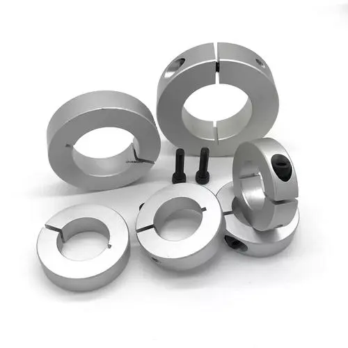
The Critical Role of Positioning Rings in Semiconductor Testing
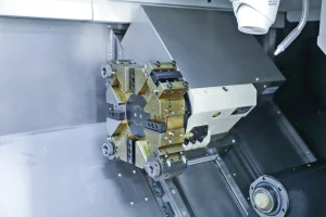
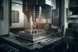
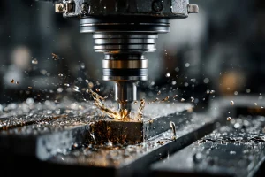
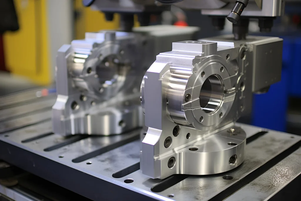
In the world of semiconductor testing, CNC Machining Test Positioning Rings is a critical process that ensures perfect alignment between the probe card and the wafer. Even a micron-level offset can lead to false failures, damaged probes, or decreased yield.
В Быстроэффективный, we specialize in machining these high-precision components using advanced materials that withstand repeated thermal cycling and mechanical stress.
Technical Comparison: Why Precision Matters
| Особенность | Standard Positioning Rings | Rapidefficient High-Yield Grade |
| Толерантность (Параллелизм) | $\pm 0.02$ мм | Ultra-precise $\pm 0.005$ мм |
| Material Choice | Standard Aluminum | ПЭК, Torlon, or Stainless Steel 316L |
| Surface Hardness | Varies | Specialized coatings for wear resistance |
| Dimensional Stability | High thermal expansion | Stress-relieved for zero-drift operation |
Key Engineering Advantages of Our Process
1. Micron-Level Concentricity and Flatness
For a positioning ring, flatness is everything. If the ring is warped, the entire test nest becomes slanted.
- Наше решение: We use a specialized “low-stress” milling strategy, similar to our approach for thin-walled parts, ensuring the ring remains perfectly flat even after intensive machining.
2. Advanced Material Expertise
Different test environments require different thermal properties.
- Our Expertise: We machine rings from ПЭК for chemical resistance, Torlon 4203 for high-strength electrical insulation, и Нержавеющая сталь for maximum durability. This mirrors the micron-level precision we provide for optical systems.
3. Enhancing Test Efficiency and Longevity
A ring that wears out quickly causes downtime.
- Наше решение: We offer specialized surface treatments, such as hard-coat anodizing or electroless nickel plating, to ensure the ring maintains its dimensions over millions of test cycles. This is the same semiconductor-grade reliability found in our wafer carrier solutions.
Why Partner with Rapidefficient?
- Zero-Defect Quality: 100% CMM inspection for critical dimensions.
- Быстрое прототипирование: 3-5 day lead times to support your R&D cycles.
- Technical Support: DFM feedback on material selection and tolerances.
Need high-precision test positioning rings?
[Contact Our Engineering Team for a DFM Review] or explore our [Услуги по обработке с ЧПУ] for more precision solutions.