The Critical Function of Bushings in Wafer Processing
In the ultra-clean environment of a semiconductor fab, CNC machining semiconductor bushings is a high-stakes task. These components often serve as critical alignment guides or thermal insulators within vacuum chambers. Any microscopic burr or material impurity can lead to outgassing, particle contamination, 最终, thousands of dollars in lost wafer yield.
在 快速高效, we move beyond standard machining to provide semiconductor-grade reliability through advanced DFM (制造设计) and rigorous cleaning protocols.
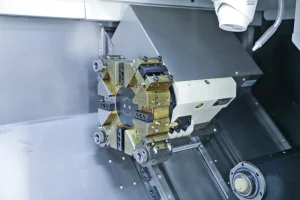
(Caption): “Our CNC facility is equipped to handle complex semiconductor geometries, ensuring that every bushing meets stringent micron-level concentricity and surface finish requirements.”
Technical Specifications: Semiconductor vs. Industrial Grade
| 特征 | Industrial Grade Bushings | Rapidefficient Semiconductor Grade |
| 厚度 (OD/ID) | $\pm 0.02$ 毫米 | $\pm 0.002$ 毫米 (Ultra-Precision) |
| Surface Roughness | $拉 \ 1.6 \ \mu m$ | $拉 \ 0.2 \sim 0.4 \ \mu m$ (Diamond-Tooled) |
| Material Integrity | Standard Batch | Certified PEEK / Torlon / 316l (Traceable) |
| Cleaning Protocol | Basic Degreasing | 5-Stage Ultrasonic & Vacuum Drying |
Engineering Standards for Semiconductor Vacuum Environments
To ensure zero-contamination in wafer processing, our CNC process for bushings adheres to the following critical metrics:
- Outgassing Control: 100% silicone-free machining environment to prevent volatile organic compound (VOC) contamination.
- Dimensional Stability: 24-hour thermal stabilization cycle between roughing and finishing to eliminate “creep” in high-performance polymers.
- Zero-Subsurface Damage: We utilize sequential diamond-tooling to achieve ultra-low roughness without abrasive polishing, which can trap unwanted particles.
Why Do Standard CNC Bushings Often Fail in Semiconductor Equipment?
Most general-purpose CNC shops fail to meet semiconductor standards due to three hidden factors:
- Thermal Creep: Polymer bushings (like PEEK) have high coefficients of thermal expansion. If not “heat-stabilized,” they will shrink or expand once installed in a vacuum chamber, leading to critical alignment failure.
- Subsurface Damage: Aggressive cutting parameters can cause micro-cracks. These cracks act as “dirt traps” for particles, ruining cleanroom ISO class integrity.
- Cross-Contamination: Machining semiconductor parts on machines previously used for lead or copper-heavy alloys leads to metallic ion contamination on the wafer.
Core Strategies for Machining High-Performance Bushings
1. Material Selection for Zero-Contamination
Semiconductor environments involve corrosive gases and extreme temperatures. We specialize in machining bushings from 窥视 (Victrex 450G), Torlon 4203/5030, and high-purity Stainless Steel 316L. Each material is selected to prevent outgassing, mirroring the standards used in our wafer carriers (Internal Link).
2. Precision Concentricity and Thin-Wall Stability
Many semiconductor bushings feature thin walls to minimize heat transfer.
- Our Solution: We utilize specialized “single-pass” boring techniques and custom expansion mandrels to maintain concentricity within $\pm 0.005$ 毫米, adapted from our strategies for thin-walled parts (Internal Link).
3. Surface Integrity and Ultrasonic Cleaning
For semiconductor applications, the surface finish is about preventing particle entrapment. Every CNC machining semiconductor bushings project concludes with multi-stage ultrasonic cleaning and inspection under high-magnification scopes, identical to our test positioning rings (Internal Link) 质量控制.
🚀 Case Study: Solving Deformation in Ultra-Thin PEEK Bushings
The Challenge:
A leading manufacturer required a batch of PEEK semiconductor bushings with a wall thickness of only 0.5 毫米 and a concentricity requirement of $\pm 0.01$ 毫米. Standard methods resulted in a 40% rejection rate due to material “creep.”
Our Engineering Solution:
- Thermal Stabilization: Implemented a 24-hour heat-soak cycle to relieve internal stresses.
- Custom Tooling: Designed a custom internal expansion mandrel to provide 360-degree support during boring.
- Cryogenic Cooling: Utilized specialized air-cooling to keep the tool-tip temperature constant.
The Result:
The final inspection showed a 100% pass rate, with concentricity held at a consistent 0.006 毫米—exceeding the client’s original specification and ensuring a perfect vacuum seal.
Technical FAQ: Semiconductor Bushing Machining
Q: What are the best materials for semiconductor bushings?
一个: For high-temperature and plasma environments, 窥视 (Victrex 450G), Torlon 4203/5030, and Stainless Steel 316L are industry standards due to their low outgassing and high thermal stability.
Q: How do you ensure zero-contamination for vacuum chamber use?
一个: We use non-silicone coolants during machining, followed by a 5-stage ultrasonic cleaning process in a controlled environment to remove all microscopic particles and residues.
Q: What is the tightest tolerance achievable for PEEK bushings?
一个: Depending on the geometry, Rapidefficient can maintain tolerances as tight as $\pm 0.002$ 毫米 by utilizing specialized fixtures, diamond tooling, and environmental temperature control.