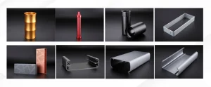
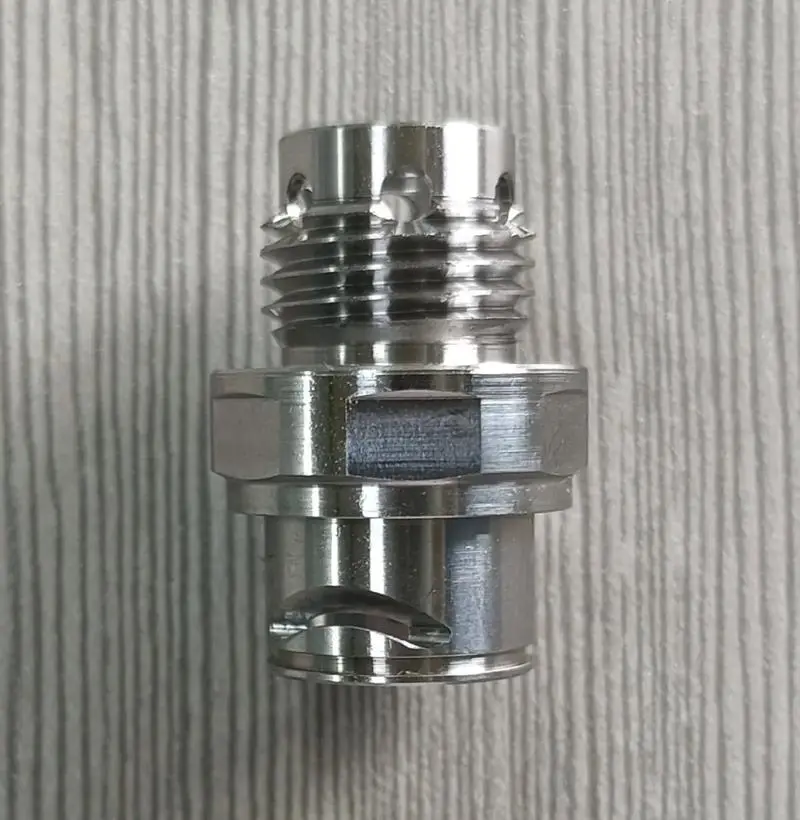
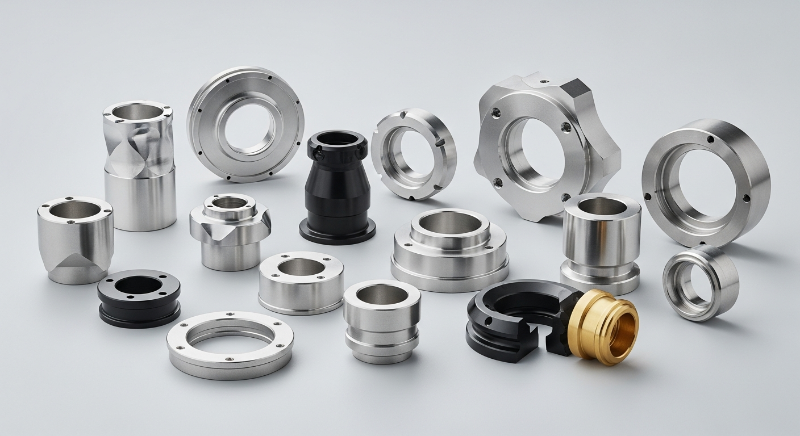
In semiconductor manufacturing equipment, adapters serve as critical connectors in vacuum chambers, gas delivery systems, and wafer handling modules. Their machining quality directly affects system cleanliness, sealing performance, and long-term operational stability.
Unlike conventional industrial components, semiconductor adapters require not only ultra-high dimensional accuracy but also strict control over surface roughness, material purity, and residual stress. At 快速高效, we approach semiconductor CNC machining with a process-driven methodology—from DFM optimization to controlled production and final inspection—to ensure consistent and reliable results.
1. Material Selection for Semiconductor CNC Machining
Semiconductor environments typically involve:
- High vacuum conditions
- Corrosive gases
- Thermal cycling
This places strict requirements on material performance.
Common materials include:
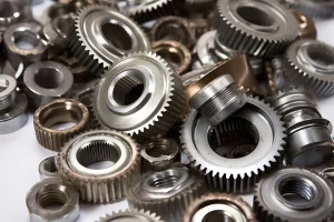
- AL7075-T6 aluminum alloy
High strength and lightweight, but sensitive to anodizing consistency - SUS316L stainless steel
Excellent corrosion resistance and vacuum compatibility - Nickel-based alloys (例如。, 铬镍铁合金 718)
Suitable for extreme environments but difficult to machine
To ensure material reliability:
- Raw materials are sourced from verified suppliers
- Incoming materials are verified for composition and consistency
- Trial processes (例如。, anodizing validation) are conducted before mass production
For difficult-to-machine alloys, cutting strategies and coolant control are optimized to minimize thermal deformation and ensure dimensional stability.
2. Precision Control and Deformation Management
Semiconductor adapters often feature:
- Thin-wall structures
- Multi-hole configurations
- Tight positional tolerances (typically ±0.005–0.01 mm)
To achieve stable precision:
- Roughing and finishing are separated
- Controlled machining allowance is applied
- Stress relief processes are introduced when necessary
Through early-stage DFM analysis, we work with customers to:
- Optimize wall thickness ratios
- Improve tool accessibility
- Reduce machining risks
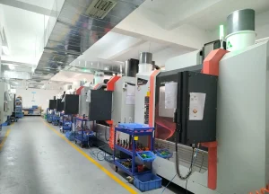
Using 3+2 machining and 5-axis CNC systems, multi-surface and multi-hole features can be completed in a single setup, significantly reducing cumulative errors.
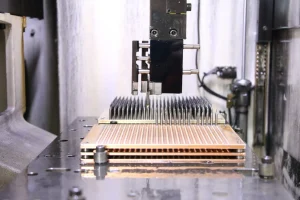
3. Advantages of 5-Axis CNC Machining
Modern semiconductor adapters increasingly include:
- Complex flow channels
- Non-standard geometries
- Multi-directional hole structures
5-axis machining provides key advantages:
- Maintains optimal tool orientation
- Improves surface finish (Ra 0.4–0.8 μm achievable)
- Enhances contour accuracy
此外, optimized toolpaths enable:
- Reduced burr formation
- Improved internal feature quality
- Less manual intervention
This is particularly important for parts used in vacuum environments where contamination must be minimized.
4. Surface Treatment and Cleanliness Control
For semiconductor components, surface quality is directly related to contamination risk.
Key considerations include:
- Controlled surface roughness
- Particle reduction
- Consistent surface treatment
For anodized aluminum parts:
- Dimensional compensation is considered during machining
- Typical anodizing growth is controlled within 0.008–0.012 mm per side
To ensure cleanliness:
- Parts undergo controlled handling after machining
- Surface defects such as scratches or dents are strictly avoided
- Inspection processes focus on both dimensional accuracy and surface integrity
5. Quality Inspection System
Precision verification is critical in semiconductor CNC machining.
Our inspection system includes:
- CMM (Coordinate Measuring Machine)
- Cylindricity and geometric tolerance testing
- Surface inspection and defect control
Each part is verified before shipment to ensure compliance with customer specifications and semiconductor industry requirements.
6. DFM Optimization for Cost and Efficiency
Cost efficiency in semiconductor machining is achieved through process optimization rather than compromising quality.
Typical DFM recommendations include:
- Avoiding deep, small-diameter holes
- Reducing unnecessary tight tolerances in non-critical areas
- Optimizing geometry for machining efficiency
Through early-stage DFM collaboration, customers can:
- Reduce machining time
- Improve yield
- Achieve more stable production
7. Production and Delivery Capability
For international customers, stable delivery is essential.
快速地:
- Prototype lead time: typically 3–7 days depending on complexity
- 小批量生产: 灵活的
- 量产: consistent quality and repeatability
Our focus is on reliable delivery aligned with project requirements, rather than unrealistic speed claims.
常问问题
How is vacuum compatibility ensured?
By controlling material quality, minimizing contamination during machining, and applying appropriate cleaning and surface treatments.
What machining accuracy can be achieved?
Critical tolerances can typically be controlled within ±0.005–0.01 mm, depending on geometry and material.
How are anodizing inconsistencies managed?
Through controlled material sourcing, pre-production validation, and process parameter optimization.